

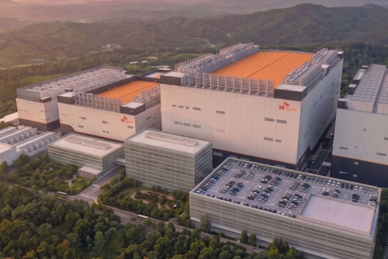
SK hynix has approved a $38.3bn investment in the construction of two new semiconductor fabrication facilities in South Korea.
The investment follows earlier plans from South Korea leaders to invest $880bn in semiconductors, physical AI and AI data centres, and a new Yongin Semiconductor Cluster hub in the southwest of the country.
Within the specifics of the $880bn plan, both Samsung and SK Hynix plan to build multiple new facilities in the new hub outside of the capital city of Seoul.
The $38.3bn investment covers a new Yongin Y2 fabrication plant at the Yongin Semiconductor Cluster and a further NAND flash facility at an existing SK hynix manufacturing site.
The specifics of the Yongin Y2 fabrication plant
Yongin Y2 will be the second of four semiconductor fabs planned by SK hynix at the Yongin cluster, located south of Seoul.
Construction is scheduled to begin in July 2027, with the facility’s first cleanroom due to become operational in June 2029.
The fab will manufacture DRAM products, including high-bandwidth memory, which is used in AI and other high-performance computing applications.
Once complete, the facility will have 279 acres of floor space, according to the announcement.
The specifics of the NAND flash production
The second facility will focus on NAND flash production and will be constructed on a campus already home to three fabs.
The company said existing power and water infrastructure at the site is expected to support and accelerate the construction programme, with the first cleanroom scheduled to open in December 2028.
The two new fabs together represent one of the company’s largest recent investments in production infrastructure.
In March, the company also announced plans to build a fab that integrates AI, robotics and digital-twin systems by 2030, featuring next-gen cleanroom environments.


