
Tesla is set to launch its “Terafab” semiconductor fabrication facility within the next four days.
CEO Elon Musk announced on 14 March that the new site would help secure a production of custom AI chips for autonomous driving and other high‑compute applications.
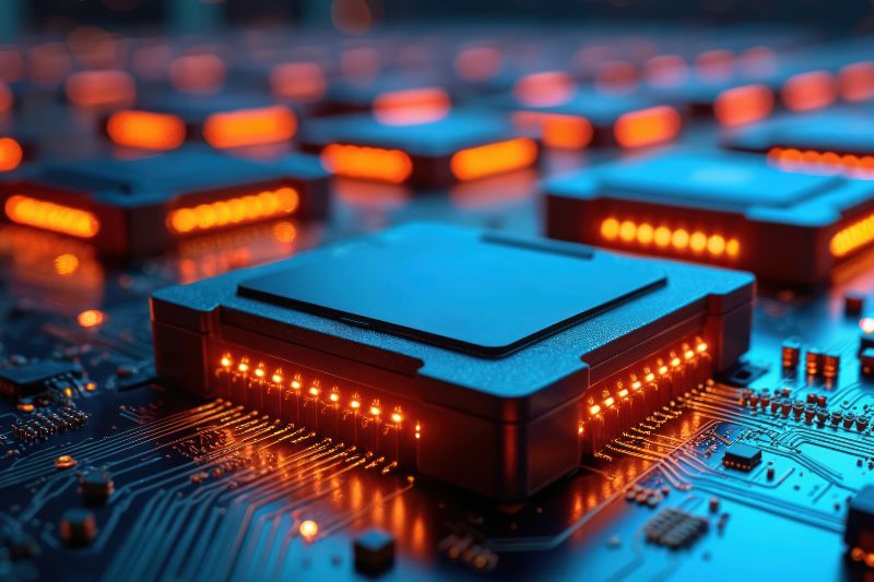
The facility represents a significant expansion of Tesla’s vertical integration into semiconductor manufacturing.
The dedicated facility, described by Musk as “gigantic,” potentially larger than Tesla’s existing Gigafactories, which themselves run into millions of square feet.
The facility is expected to support production of 100–200 billion AI and memory chips per year.
No other specific details were released, such as site location, floor area, or cleanroom size.
The move for Tesla marks a significant shift from their traditional automotive and battery production footprint into semiconductor manufacturing, a domain that requires ultraclean environments, precision process control and extensive vertical integration.
Musk has also suggested that conventional cleanroom designs may not be essential for future fabs, sparking debate about alternative wafer‑level isolation approaches.
In a recent interview, he claimed that wafers could be protected even in environments where people are present, a very different approach to current contamination control strategies.
Industry experts caution that while wafer‑level containment may reduce room-scale requirements, high‑precision fabs still depend on controlled environments to maintain yield and reliability.
As Terafab readies for its initial launch phase, the industry will be watching not only the output and timelines, but how Tesla navigates these technical challenges, particularly those at the intersection of contamination control, cleanroom engineering and wafer‑level process integrity.


