
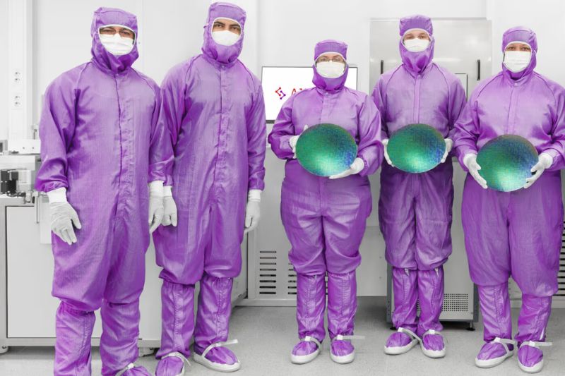
A Swedish semiconductor startup is moving to industrialise a new chip manufacturing technology in the Netherlands.
This new collaboration is designed to reduce the cost and complexity of producing advanced AI chips.
AlixLabs has signed a memorandum of understanding with VDL ETG Projects to scale its atomic-level chip patterning technology called Atomic Pitch Splitting (APS).
VDL ETG Projects is a specialised subsidiary of the VDL Enabling Technologies Group (ETG), acting as a top-tier contract machining manufacturer and development partner for high-tech equipment.
The partnership will centre on Eindhoven, reinforcing the region’s position as a key hub in Europe’s semiconductor supply chain.
What is APS, and why is it so unique?
The APS process uses atomic layer etching to split patterns at the nanoscale, enabling chipmakers to achieve finer resolutions with fewer process steps.
The approach is positioned as an alternative to increasingly complex and costly multi-patterning techniques and extreme ultraviolet (EUV) lithography.
The technology has the potential to replace up to five conventional manufacturing stages with a single step.
This offers both cost and energy efficiencies in semiconductor fabrication.
AlixLabs said its technology could allow existing semiconductor fabrication plants to be upgraded to produce AI chips, avoiding the need for new facilities that can cost up to €20bn (about £17.4bn) to build.
The company is currently in discussions with potential customers in Asia and aims to install its first machines for testing in 2027, with full-scale production targeted by 2029.
Benefits of the collaboration
The collaboration will see VDL ETG Projects take a leading role in translating the technology into industrial-scale equipment, supporting AlixLabs’ transition from research and validation to commercial deployment.
The origins of APS date back to 2015, when AlixLabs’ founder, Jonas Sundqvist. identified the potential of an unexpected experimental outcome while working at Lund University’s Nano Lab.
The discovery led to the development of a method capable of producing finer chip features through controlled material splitting at the atomic level.
“This MoU represents an important milestone for AlixLabs as we move from technology validation toward industrial deployment,” said Jonas Sundqvist, CEO of AlixLabs.
Sundqvist said that the partnership with AlixLabs to scale its APS technology will bring a new patterning paradigm to the semiconductor industry.
Sorin Stan, Senior Director for Emerging Technologies at VDL ETG Projects, said that the first industrial version of the APS machine is currently being developed, and that AlixLabs could become part of how chipmakers plan and upgrade future advanced semiconductor manufacturing processes.
“The implementation of AlixLabs’ research in the manufacturing processes for advanced semiconductor devices will contribute to overall cost reductions and increased production speeds,” said Stan.
The initiative is supported by European investment, including backing from venture capital firm ForwardOne, and guidance from industry figures such as Arthur van der Poel.


