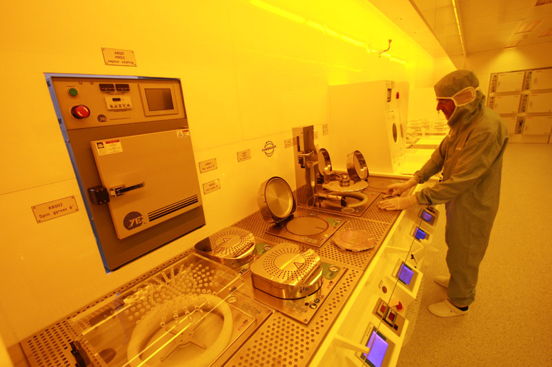
The cleanroom at the Binnig and Rohrer Nanotechnology Center in Zurich, Switzerland, is unique; it has been specially designed to accommodate research for micro and nanofabrication. What's more, the site is equipped with a noise-free lab for product characterisation.
A close collaboration between IBM Research and the university ETH Zürich, the centre started operation in May 2011 following a US$90m investment. The 950sqm state-of-the-art cleanroom was outfitted quickly and operation ramped up in the first 1.5 years.
Now in full swing, IBM Research scientists and ETH staff and students work side-by-side on the groundwork for next-generation technology. “What we do is [research] on micro and nanofabrication for silicon, III-V compounds, and other materials with a focus on microelectronics,” tells me Dr Roland Germann, the Operations Manager of the centre.
The cleanliness of the air is an important, if not the most critical element for the operation of the centre. “We are building nanostructures of 10 nanometres and below, and for that, you really have to get rid of particles,” Germann enthuses. Put it in context, one nanometre is a billionth of a metre; that's 75,000 times smaller than the average width of a human hair of 75 microns.
Cleanroom design
The facility features a bay-chase layout, a concept utilised in many R&D buildings. Here, individual cleanrooms, which are small rooms within the room, are surrounded by a service area. The wafer processing and handling take place inside the cleanroom bays and these range from ISO Class 100 (ISO 5) to ISO Class 10,000 (ISO 7). The service area, or grey room, houses auxiliary equipment and is used to connect the tools to all necessary media: electricity, water, gases, ventilation, etc.
The operation of the cleanroom is user-led. “Students and researchers from IBM and ETH come to the cleanroom and they perform their work on their own,” Germann says. And for them to work efficiently, training is key and includes a general introductory class that teaches the basics of cleanroom technology: how to dress up and dress down, including how to use the overall and other PPE, and how to behave in the cleanroom to prevent contamination risks.
Users also must pass training on the use of the tools. “Step by step, they learn how to do things in the cleanroom and how to keep the cleanroom in a clean condition,” Germann points out.
Training, he says, is crucial because the way people work can create more or fewer particles. He explains: “We use special cleanroom-ready pen and papers, and it is really to protect the samples. We work with nanoscale structures; a speck of dust is much larger than the feature you are trying to produce! That’s why it is important to keep the environment clean.”

Temperature and humidity are also important environmental factors to control; if they fluctuate too much certain tools would not work as expected. “For pattern definition we use photoresists, which are very sensitive; too much humidity and the resist layers would not stick to the surface of the wafers; if there is not enough humidity some chemical processes would not function correctly. Humidity is controlled to around 45%, for that reason,” he explains. Temperature, on the other hand, is kept at around 20-22°C.
The cleanroom is lit by yellow lights for a fundamental manufacturing reason. Germann explains: “To define the patterns you want to produce [on wafers] a technology called lithography is used, which works like good old photography: you have a layer in the wafer that is sensitive to light and an image is projected onto this layer thereby the pattern is defined. The photoresist we use are sensitive to blue light, so the ambient light would expose that photoresist and change its properties. As the blue light is banned, we use the yellow filter.”
Freedom to experiment
Creating the supercomputer of tomorrow challenges scientists to design chips that mimic the efficiency of the human brain. After all, the market trend is toward faster processing of large volumes of data with better battery life.
Dr Kirsten Moselund and her team of IBM researchers use the cleanroom for projects with novel materials integrated on silicon for ultra-low power electronic devices, among other studies. Her work focuses on the integration of III-V heterostructures on silicon.
“This is not a conventional CMOS production facility; it is really a nanotech centre; this allows us to try out things that we can’t do in a process line,” she tells me. Moselund says the team can work with exotics materials that can’t be introduced to semiconductor foundries because of contamination risks.

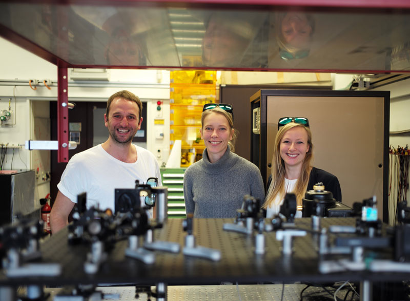
Dr Kirsten Moselund and her team of IBM researchers use the cleanroom for projects with novel materials integrated on silicon for ultra-low power electronic devices
Bringing in novel materials to a production line risks contaminating a process that has been established over years. With the centre, IBM has a facility that allows staff to experiment. Moselund comments: "We can try making new devices that potentially could be better than those we have on silicon. Also, here we have a very high concept level; we have access to a very high-resolution e-beam, for example. With the tools, we can do something that is close to what can be done in a production facility, but with different materials."
An excellent electronic medium, silicon (Si) is today the most used semiconductor material; is abundant, low cost and robust. But, III–V materials provide several advantages over Si.
A III-V compound semiconductor is an alloy containing elements from groups III and V in the periodic table. Their advantages over Si include lower effective masses, higher mobilities and a direct bandgap, which renders them more suitable for both photonic and tunnelling devices. “For example, you can make lasers from these materials, something you can’t do with silicon. Also, depending on the compound, you can make faster and low-powered transistors,” she says.

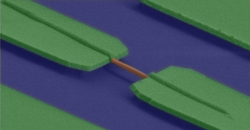
Tiny wires made of III–V materials promise to be an essential component for the semiconductor industry. Photo IBM Research
ETH scientists and students work on different semiconductor-based processes with materials including germanium, carbon, graphene, metals, insulators, polymers, organics and oxides.
The cleanroom is equipped with tools to process these materials at the nanometre scale; wafers from 6-inch up to 200mm in size. The tooling available ranges from optical lithography, wet processing and thin film deposition. The machinery also includes dry etching and thermal processing. There is also a metrology and inspection sector and a carbon deposition sector, to name but a few.
Noise-free lab
Work in the centre leads to prototype devices that manufacturers might be using in the future. Because this is research work at the nanometre scale, scientists require accuracy at the same level; here is where the noise-free lab comes to play.“We have designed laboratories where we have tried to ban mechanical vibrations completely, tried to minimise electromagnetic fields, acoustic noise and we tried to make them temperature stable,” Germann explains. The infrastructure comprises six research labs with a total floor space of 176sqm located in the basement of the building.
One can’t really weigh the breadth of applications that are in the making at the centre. People in the cleanroom work in the field of MEMS, optical communications, new materials like carbon, TMDCs; microfluidics for health application; you name it. Germann comments: “It is very astonishing for me to see how many different things are done in the cleanroom by all our users. It goes beyond IBM's traditional activities of building microprocessors.”
An example of the capabilities of the centre is work recently completed following a five-year research with III-V CMOS and III-V phologics (nanophotonic logic gates). Both developments, Moselund tells me, really pushed the capabilities of the cleanroom to the limit. “We demonstrated the integration of multiple layers of logic (undelaying of logic that is silicon-based and then putting III-V devices on top with a state-of-the-art resolution). It is not yet a commercial product, but it is the direction we would like to go,” she concludes.
IBM Research took home the 2017 Compound Semiconductor Industry Innovation Award for that project; no doubt further breakthrough is yet to come. www.zurich.ibm.com/brnc
N.B. This article is featured in the December 2018 issue of Cleanroom Technology. The digital edition is available online.
