Forge Nano has announced the completion of an ISO Class 4 cleanroom for production of its new semiconductor manufacturing tool launched in 2024.
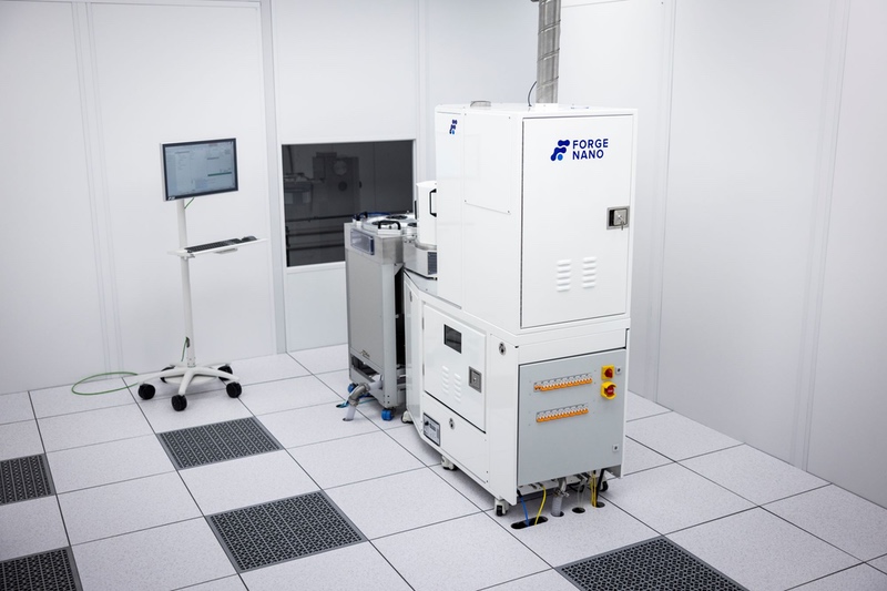
The new TEPHRA is an ALD cluster tool. Atomic layer deposition, or ALD, is a manufacturing approach that deposits materials and films in exact places.
As a cluster tool, TEPHRA is dedicated to high volume manufacturing of speciality semiconductor applications on 200 mm wafers and below.
The US-based semiconductor expert and atomic layer deposition solution provider has opened the new 2,000 sqft cleanroom to manufacture multiple commercial TEPHRAs.
The company states that this expansion was necessary to accommodate growing equipment demand.
The remainder of the cleanroom will serve as a dual operating space for demonstrations and manufacturing
The new cleanroom provides an ISO Class 4 space for processing sensitive customer samples and includes a metrology lab for advanced thin-film measurement and particle inspection.
The remainder of the cleanroom will house Forge Nano’s own internal TEPHRA tool and provide space to build multiple customer tools, serving as a dual operating space for demonstrations and manufacturing.
In addition to increased manufacturing space, this expansion is poised to accelerate Forge Nano’s ability to provide proof-of-concept and commercial solution validation to manufacturers planning to integrate new ALD processes.
Matt Weimer, Director of R&D at Forge Nano, said: “With this new cleanroom, Forge Nano will be able to showcase the capabilities of our ALDx atomic layer deposition processes to our customers and further our solutions for advanced packaging and 3D chip integration.”


