Southampton University has launched its new E-beam lithography suite.
Japan, once a leader in semiconductor manufacturing, now plays a pivotal role in the global semiconductor supply chain through its dominance in essential materials and equipment.
In the last week, the first 200 kilovolt (kV) system outside of Japan was installed at the University of Southampton. Major Japan-based instrument manufacturer JEOL sold its JBX-8100 G3 for use in the facility.
This instrument is used to perform E-beam lithography. Semiconductor lithography is a crucial process in making microchips and other semiconductor devices. It involves using light or other forms of radiation to transfer intricate patterns onto a silicon wafer. These patterns are what allows the semiconductor to function.
Specifically, E-beam (Electron-beam) lithography uses a focused beam of tiny particles called electrons to create patterns in materials with unrivalled resolution – allowing researchers to create features thousands of times smaller than a human hair.
The technology can be instrumental in enabling manufacturers to create the tiny components that power technologies of the future, from medical diagnostics to defence systems.
The facility
The new E-beam lithography suite, which contains the landmark system, is now housed in the Kepler Cleanrooms at the Optoelectronics Research Centre (ORC).
The Zepler Cleanrooms Complex is a science centre that includes a variety of facilities and laboratories for materials and device research in electronics, photonics and nanotechnology, with both planar wafer and optical fibre capabilities supporting both research and enterprise.
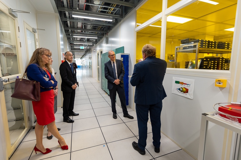
UK Science Minister Lord Vallance opened the new facility at the end of April 2025 alongside University Vice-Chancellor Professor Mark E. Smith and Professor Graham Reed, who leads its ORC and CORNERSTONE. The ceremony also welcomed Osamu Wakimoto, Executive Officer from Jeol Japan to celebrate the occasion.
Professor Graham Reed said: "The introduction of the new E-Beam facility will reinforce our position of hosting the most advanced cleanroom in UK academia.”
The role of the UK
Southampton University stated in a release that a single semiconductor worker contributes an average £460,000 to the UK economy per year.
The semiconductor industry in the UK, like Japan and much of the world, is in a state of evolution. For the UK, its part hinges on research and innovation, as well as niche applications, as opposed to mass manufacturing. The University of Southampton is part of this innovation focus, and the cleanrooms at this facility are enabling this to happen.
Image credit: Southampton University


