L&K Engineering, a China-based mechanical and electrical engineering construction company, has won a major contract to provide engineering services to VisionPower Semiconductor Manufacturing Company.
The contract is worth ¥630m (Chinese Yuan).
VisionPower Semiconductor Manufacturing Company is a new 300mm semiconductor wafer manufacturing facility to be built in Singapore.
The new facility is a joint venture between Vanguard International Semiconductor and NXP Semiconductors.
The contract is worth ¥ 630,000,000 (Chinese Yuan)
Vanguard International Semiconductor is a Taiwan-based specialty Integrated Circuit foundry (IC) foundry service provider that mainly manufactures and offers semiconductor solutions in areas such as mixed-signal, power management, and analog devices.
NXP Semiconductors is a Netherlands-based semiconductor manufacturer most known for developing secure connectivity solutions for embedded applications for the automotive, industrial IoT, mobile, and communication infrastructure industries.
This joint venture aims to build and operate a 300mm semiconductor wafer manufacturing facility in Singapore.
The facility will focus on producing mixed-signal, power management, and analog products for markets such as automotive, industrial, consumer, and mobile devices.
Construction of the fab is set to begin in the second half of 2024, with production planned to start in 2027
The technology for this fab will be licensed by Taiwan Semiconductor Manufacturing Company (TSMC), a leader in semiconductor manufacturing.
Construction of the fab is set to begin in the second half of 2024, with production planned to start in 2027.
The fab will eventually reach a capacity of 55,000 wafers per month by 2029, and the project is expected to generate around 1,500 jobs in Singapore.
The total investment in the initial phase is estimated at $7.8bn (US dollars), with VIS holding a 60% stake and NXP 40%.
The facility will focus on producing mixed-signal, power management, and analog products for markets such as automotive, industrial, consumer, and mobile devices
This joint venture aligns with both companies' strategies to diversify and expand their manufacturing capabilities, ensuring competitive costs and supply chain resilience.
VIS Chairman. Leuh Fang, said: "VIS is pleased to work with leading global semiconductor company NXP to build our first 300mm fab. This project aligns with our long-term development strategies, demonstrating VIS’ commitment to meeting customer demands, and diversifying our manufacturing capabilities"
NXP President and CEO, Kurt Sievers, said: "We believe VIS is well suited and fully understands the complexities involved in building and operating together with NXP a 300mm analog mixed signal fab. The joint venture partnership we intend to create with VIS perfectly aligns with NXP’s hybrid manufacturing strategy."
In terms of sustainability, this fab will be built adhering to the Singapore Green Mark standards and implementing rigorous green manufacturing measures, according to Vanguard International Semiconductor.
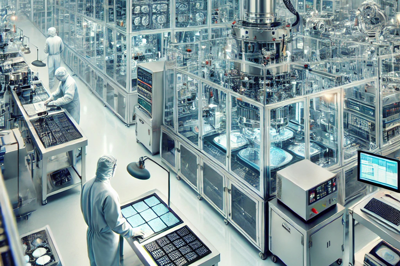
Top image: AI-generated image depicting semiconductor manufacturing inside a cleanroom environment. The scene shows workers in full protective suits managing advanced machinery, like photolithography and wafer-handling equipment, ensuring the precision and cleanliness necessary for producing high-tech semiconductor wafers.


