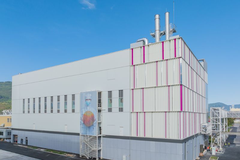
CEA-Leti has officially inaugurated the FAMES Pilot Line, featuring a 2,000 sqm cleanroom.
The facility, which expands CEA-Leti’s total cleanroom space to 14,000 sqm, is designed to support the development and prototyping of advanced FD-SOI, RF, embedded memory, 3D integration, and power management technologies.
What is unique about the new cleanroom?
The facility is open-access, enabling European startups, SMEs, industrial groups, and research organisations to prototype, qualify, and de-risk cutting-edge semiconductor technologies before industrial deployment.
The cleanroom houses more than 80 of the most sophisticated 300mm tools in the industry.
Two basement levels manage complex technical installations, while a five-meter ceiling height accommodates large-scale equipment.
Low vibration levels and dedicated electrical backup systems ensure uninterrupted operation, critical for precision semiconductor fabrication.
“The breakthrough technologies developed within FAMES are intended to support future generations of sub-10 nm FD-SOI chips, enabling high-performance and low-power components for Europe,” said Jean-René Lèquepeys, Deputy Director and CTO of CEA-Leti.
More than 350 representatives from industry, research organizations, public authorities and European institutions gathered for the inauguration of the cleanroom.
Environmental sustainability was also a key consideration in the cleanroom design.
The building incorporates high-performance insulation and systems for waste-energy recovery, optimising its environmental footprint while maintaining the stringent conditions required for semiconductor manufacturing.
“This cleanroom represents the heart of our ‘lab to industry’ model and is fully aligned with the ambitions of the Chips Act, securing innovation and technological sovereignty in microelectronics,” said Anne-Isabelle Etienvre, Director General of the CEA.