Many organisations are looking to nanotechnology research for tomorrow’s products; IBM aims to make its Nanoscale Exploratory Technology Lab one of the most advanced facilities. Susan Birks reports.
Nanotechnology is a field of science that is leading to new products and hi-tech manufacturing processes. IBM is one of many multi-nationals looking to exploit this science to develop tomorrow's business solutions. To help reach this goal, IBM is building a new facility – the Nanoscale Exploratory Technology Lab (NETL) – for exploratory research. A range of fields will be pursued, including: MEMS/NEMS, spin-tronics/magnetism, nanowires, carbon-based devices, functional materials, directed self-assembly, electronic packaging, thermal management, 3D integration, optical inter-connects, photonics, nanobiology and simulation.
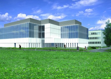
IBM Research – Zurich is teaming up with the Swiss Federal Institute of Technology Zurich to establish this ultramodern facility. The NETL is being built on the IBM campus in Rüschlikon, Switzerland, and is planned for completion in spring 2011. It will cover some 6,000m2, of which 900m2 will be dedicated to cleanrooms, and it is costing around CHF90m (€61m), of which CHF30m (€20.4m) is being spent on infrastructure.
It will have specialised 'noise free' labs that cater for work with electronic products and technologies at the nanoscale. The cleanrooms, meanwhile, will feature class 100/1000 facilities with class 10 mini-environments, designed to accommodate processes such as lithography, wet processing for substrate cleaning and chemical etching, thin-film deposition, dry etching, thermal processing for oxidation, annealing and vapour phase deposition, metrology/inspection with optical and electron microscopes, as well as back-end processes such as plating, lapping/polishing, dicing and bonding and polymer waveguide processing for optical interconnects. These processes, most of which will be semiconductor-based (silicon, III/V), will be conducted on materials similar to those used in standard semiconductor technology, such as silicon, metals, isolators, polymers, organics and oxides.
Because nanotechnology experiments are extremely sensitive, the labs must be insulated as much as possible from external disturbances, such as detrimental vibration-acoustic effects (external and internal traffic, elevator operation, vibrations caused by persons entering the lab, etc.), low-frequency magnetic fields and fluctuations in room temperature.
Each of the six labs has approximately 250ft2 (23.2m2) of floor space, allowing the operation of highly sensitive measurement equipment and tools. The challenging specifications targeted for these facilities will be achieved by a variety of cutting edge measures, including a triple insulation concept.
To minimise vibration-acoustic disturbances, every lab will have its test bench mounted on seismic blocks with pneumatic damping. In addition, the test benches will be installed on double-floored bases to eliminate vibrations. Thus the separated tool platform will be vibro-acoustically decoupled from the building and operator platform. A massive concrete pedestal (> 65 tons), will suppress frequencies above 25Hz. The tool platforms will have passive mechanical damping, suppressing frequencies above 3Hz. There will be active mechanical damping down to 0.5Hz.
Electro-magnetic fields are another possible disruptive factor and must be kept below 5 nano Tesla (nT), which is 1/10000 of the Earth’s magnetic field. Therefore, laboratories will be insulated by passive and active shielding. Passive shielding is achieved by the use of continuous metal sheets as wall and ceiling covering. Moreover, there is no connection between the floor and wall shielding. This passive shielding protects against permanent external electromagnetic fields, such as those from the train tracks, as well as against temporary fields originating in neighbouring labs. The passive mu-metal shielding of each lab to screen external EMF will reduce EMF within the lab to B < 20nT. An active control system consisting of inductor pairs will also be installed. This EMF cancellation system, consisting of three pairs of Helmholtz coils, will cancel the remaining EMF and guarantee B < 5nT.
Humidity and temperature control are both key to many of the advanced manufacturing processes mentioned. For this reason the facilities will have a distributed, homogeneous-flow HVAC system that will keep temperature fluctuations to a minimum. An intricate system of air recirculation will be deployed to keep the temperature stable at 20–26°C (+/-0.5°C) and the humidity at 35–50% RH by means of separate adjustments of the supply and exhaust air, separate air-cooling and air-heating systems, and separation of the air ducts from air-conditioning. Moreover, in these ducts, sound absorbers and insulation will be installed to counter airborne sound. All additional sources of noise, such as pumps, transformers and power supplies, will be placed remotely in chambers adjacent to each lab.
Sustainability is one of the key criteria in the construction of the lab and IBM has decided to adopt the voluntary minimum energy standard (MINERGIE), a Swiss building standard that encompasses the optimal use of renewable energy, while enhancing the quality of the working environment and decreasing its environmental impact. As a result, the building will use energy-optimised materials and state-of-the-art insulation. The MINERGIE limit for the laboratory is 40kWh/m2a – around half of what a conventionally built research building would use. Renewable energy will be provided by a photovoltaic power system and a geothermal heat exchange system; these will produce 41kW of electrical power that will be fed directly into the power supply. The facility's heat-recovery and cutting-edge HVAC systems will help reduce energy use. There will also be a transition from using oil to switching to gas.
Specification for the new NETL facility • Mechanical vibrations: Velocity less than 500nm/s (x, y, z), below 16Hz and less than 100nm/s above the 16Hz band • Acoustic noise: Sound pressure level in a 1/3-octave RMS bandwidth spectrum not more than 50dBC between the 31.5Hz and 100Hz band and less than 55dBC above the 100Hz band • Electromagnetic fields (EMF): Flux density less than B = 5nT RMS in an integral spectrum between 0 and 625Hz • Noise power: < 10-12V2RMS up to 1kHz without 50Hz < 10-10V2 RMS up to 1kHz for 50Hz and harmonics < 10-10V2RMS above 1kHz • Temperature stability: 0.1°C/1hr and 0.5°C/24hr
www.zurich.ibm.com Project design – Beta Projekt Management www.beta.ch Constructor – Karl Steiner www.steiner.ch Cleanroom planning – GP-I www.gpi-ch Acoustic/vibration engineering – Stauffer Engineering www.akustik.ch Magnetic shielding – Systron EMV www.systron.ch


