Users of nanofabrication facilities often need to prepare multiple samples from a single wafer or piece of wafer for parallel processing and other experiments and analysis. The benefit? Downsizing wafers into coupons saves cost (reduced lost wafer material) and shortens process development time relative to running a single experiment on a whole wafer.
While cleaving is a dry process and also the least destructive method, it does produce particles that can contaminate the sample and the cleanroom
Because it is not practical for wafers to leave the cleanroom, samples are prepared in the clean production environment by dicing saw or cleaving. The concern, however, is that while cleaving is a dry process and also the least destructive method, it does produce particles that can contaminate the sample and the cleanroom.
The cleaving process is commonly performed by scribing the wafer surface with a diamond scribe, then breaking the wafer by hand or using a ruler or pin for leverage. This practice will create particulate contamination.
It is critical to develop a process to prepare samples in the cleanroom that does not compromise cleanliness. Developing a successful sample preparation method for the cleanroom removes the risk that wafers will be contaminated, lost or broken.
LatticeGear, the US-based scribing and cleaving specialist, has teamed up with nanofabs as it embarked on a study to determine that cleaving can be a clean process.
Janet Teshima and Efrat Moyal, the company founders, have extensive experience in the semiconductor industry. They believe that materials cleaving and scribing should be easy and fast, without requiring costly automated tools.
Operating in the market since 2012, LatticeGear’s flagship products, the LatticeAx and Flipscribe, have been designed to provide the nanofab with a dry method to cleanly downsize wafers of a wide variety of materials, shapes and sizes. According to customer feedback, these tools offer users a repeatable wafer downsizing method proven to help reduce particle contamination.
“Our needs for the 420 (LatticeAx) were based on the high number of users downsizing wafers (cleaving small pieces of wafer by hand) while in the fab, before moving samples to major process tools and or wet chemistry,” the manager of a US-based nanofabrication facility told the company.
The nanofab has many policies in place against doing this, however, the manager admitted they are difficult to enforce. “Our costs to keep and maintain cleanliness are high, and the only way to drive a change was to offer the user a way to cleanly cleave their wafers in the fab. We implemented a solution and they were glad to use it,” he said.
The manager also revealed that acquiring the LatticeAx 420 has led to a “significant reduction in particulate contamination, as most users have shifted to cleaving with this tool”.
According to LatticeGear, there are several challenges to keeping the nanofab clean:
- High number of users: most fabs employ hundreds
- Users are researchers, not sample preparation experts
- Scribing and cleaving is mainly a manual process using scribers. Success is user dependent and can produce a few or many particles
- Nanofab users are not “invested” in the facilities. They come and go
- A nanofab doesn’t have many avenues for cost reduction and it struggles to maintain costs within budget
- Benefits to clean wafer downsizing are:
- Reduced particulate contamination
- Less damage to the samples, hence more accurate results
- Reduced cost: with less need to repeat experiments, there is less scrap
- A dry process performed at room temperature, which is gentle to the wafer
Having a clean process that protects the samples leading to more accurate results is important, especially for surface analysis preparation, e-beam lithography, photonics, and a wide variety of electronic applications.
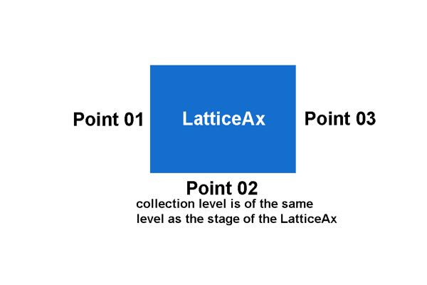
Figure 1 shows the measurement locations relative to the LatticeAx.
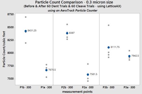
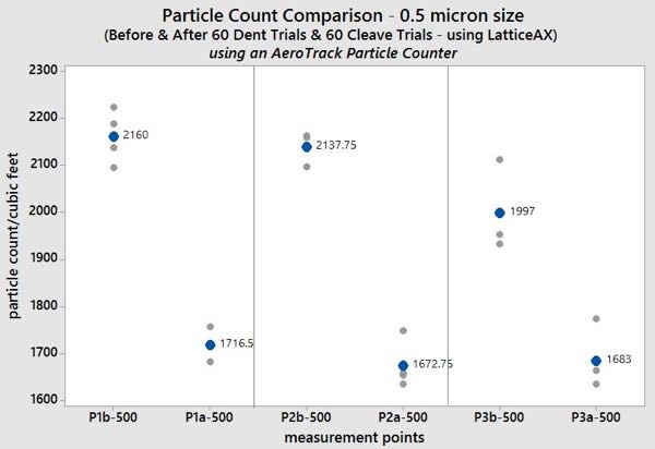
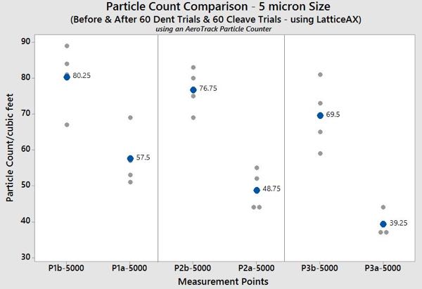
Particle collection duration was 1-minute per trial. Before and after results are reported for 0.3, 0.5 and 5.0-micron particle sizes (Figures 2-4). For all three particle sizes collected, no additional particles were added as a result of the LatticeAx cleaving process. Measurements after cleaving were always lower than before cleaving.

Figure 1: Locations of collection points relative to the LatticeAx
Problem solved
All the above issues, the company said, have been addressed in the design of the LatticeAx. A notable feature is that it includes both the weak point creation (microline indent) and the cleaving step in one tool.
“As a scribeless cleaving process, it doesn’t generate particles and is, therefore, the best cleaving option available for a cleanroom,” the company enthuses, adding that by eliminating hand scribing and cleaving, the LatticeAx reduces particulate contamination and cleanroom decontamination costs.
With this tool, the indent and cleave process impacts only the edge of the wafer (<1-mm), without touching the surface or the cross-sections. This approach eliminates contamination and leaves the structures and films intact.
“The LatticeAx is a dry, room temperature and gentle method and can handle small samples as well, which is usually the biggest challenge,” the company said.
Quantification of particle contribution

Figure 2: Particulate count comparison for 0.3 micron size, before and after wafer cleaving, points 1-3
LatticeGear engaged the University of Sydney with a study to quantify the particles generated during wafer downsizing using the LatticeAx 420.
Data was collected after the full process, from sample handling to cleaved wafer piece.
Results showed no increase in measured particles in the vicinity of the LatticeAx 420. Note that the particle count was relatively high because the test was conducted in a non-particle controlled environment.
The particle count was undertaken to determine whether the LatticeAx 420 cleaving system could be installed in the cleanroom without impacting particle count.

Figure 3: Particulate count comparison for 0.5 micron size, before and after wafer cleaving, points 1-3
To obtain statistics, 60 samples were cleaved out of 10 whole, 4-inch silicon wafers. The results showed no increase in particle count.
Particle counts were less after cleaving because the sample point was constant. Most of the particles were consumed by the counter on the first trial and then each succeeding trial.
Measurements were made using an AeroTrack Pro 9303 particle counting tool fully charged; this is essential for the stability of pump power and a reliable particle count.
Once charged, the counter was turned on and the laser stabilised for approximately 15 minutes. Zero check was done prior to particle count analysis to determine if the sensors were accurate. This was done for three, five-minute cycles. A HEPA filter attached on the particle inlet was used for this test.

Figure 4: Particulate count comparison for 5.0 micron size, before and after wafer cleaving, points 1-3
Regarding the tool parameters used, the pump speed was set up to 135 and four trials per location were the measurements per point. Worth noting is that pump speed is a relative value between 0 and 255. Zero is the lowest speed and 255 is the highest speed.
Commenting on these results, the company said: “It is clear that reducing cycle time and cost while developing the best processes is critical in creating new materials and products. Optimising something as basic as sample preparation of wafer coupons can help to streamline the workflow and achieve these goals.”
LatticeGear wishes to thank the University of Sydney and Penn State University for their assistance with this study:
Ethel Cabrera lagan, Process Engineer, Core Research Facilities, University of Sydney.
The Nanofabrication Lab, Materials Research Institute Penn State University.
N.B. This article is featured in the February 2019 issue of Cleanroom Technology. Subscribe today and get your print copy!
The digital edition is available online.
